Electronic designers may avoid considering electromagnetic compatibility because their exposure to electromagnetic field theory was so mathematically intensive. While mathematical models are important, focusing on the math can distract a person from appreciating the practical aspects of how electromagnetic fields behave.
In my experience, the easiest way to understand EMI is to think of water. Water seeks the path of least resistance, and water wants to return to its source.
In EM terms, what is a source? Any place where current originates. A buffer, a power supply, a driver, or even a bypass capacitor, an inductor, or ferrite bead can be thought of as a current source.
Unlike water, when electrical current flows, it generates an electromagnetic field. And the EM field that current generates in turn influences the path along which the current flows.
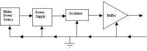
Ideally, in electronic circuits, all return currents follow paths back to their sources that match the paths that the currents originate from. Consider the diagram below:
 Figure 1: Optimal Current Paths
The arrows indicate both primary current flow paths and return current flow paths through ground. When return current flows along a path that matches the source path, the EM fields generated by the current flow cancel each other, and the circuit does not create Electromagnetic interference. Another way to look at it is that all the current energy stays within the intended pathways.
Like water, electric current energy follows the most efficient path back to its source. If the intended pathway is not the most efficient route for return current to follow, the electric fields generated by the forward and return currents will choose a more efficient path, and emissions will result.
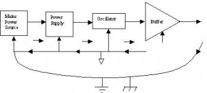
Now consider the figure below, which illustrates a problematic return path in the buffer circuit described above:
Figure 2: Problematic Current Paths
Notice in figure 2 how the most efficient return path for the current being sourced by the buffer is no longer the short path back to the buffer, but rather a long looped path through earth or chassis ground and the mains power source. When tested for emissions, the above illustration may produce either conducted or radiated emissions, depending on the frequency characteristics of the buffer sourced current.
Why would electrical energy choose a long path rather than the intended short path? This is where a little math may be required, or at least an understanding of what the math predicts. One reason might be that the longer path happens to match a resonant wavelength of some harmonic frequency of the alternating buffer current. Another reason might be that the intended return path presents a high impedance at the offending frequency and actually blocks the return current. Mismatch between the buffer circuit source, path, and destination impedances can be a factor as well, causing undesirable reflections in the buffer sourced current.
Whatever the cause for the undesirable emissions, understanding the behaviors of electromagnetic fields can help a designer to “design out” potential EMC issues prior to testing. Looking at a design as a series of current sources that require adequate return paths can assist in this understanding.
Part of our job at Sunrise Electronic Innovations includes educating our customers while doing design reviews and product pre-screen testing. As we educate our customers, their designs improve to the point that little to no modification is required for passing certification testing. To gain the benefit of our experience, please give us a call at 678-358-8775.

