In the Blog entitled Why Electronic Designs Produce EMI Part 1, we discussed why radiated emissions occur in electronic designs. A simple way to visualize electronic signal current forward and return paths was provided, and mismatched signal path impedance was briefly mentioned as one reason for signals to radiate. In this article, the significance of signal path impedance is described in greater detail.
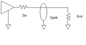
We can start by asking the question, what kind of signal path will not radiate? Mathematics aside, the simple answer is that a signal path that matches source, path, and destination impedances will not radiate. Here is a simple illustration of a matched impedance signal path:
In the above illustration, if Zin=Zpath=Zout across the entire spectrum of frequencies from DC to light and beyond, almost any signal which is sourced from the buffer will not radiate. Why not? Because all of the energy that is sourced from the buffer will be delivered to the load. What happens if there is a mismatch along the way? The simple answer is that mismatched impedances cause signals to reflect, which equates to ringing, which results in radiated noise. This is as true for high speed communications signals as it is for power supply outputs.
How much ringing will there be and at what frequencies? This depends on how much impedance mismatch occurs in the path, how much energy is being transferred, and what the resonant length of the path is.
In both high speed data and power supply applications, circuits are generally designed to have very low impedance at the source drivers, and very high impedance at the destination loads. Also in both high speed data and in power supplies, very sharp edges on switched signals are considered desirable because sharp edges with a lot of energy result in fast data transfer and maximum efficiency switching supplies. Unfortunately, these two conditions also create an ideal environment for signal reflections, especially at high frequencies.
Why do mismatched impedances reflect? Imagine a floodgate opening, and downstream a huge rock blocking the river. What will happen when the current reaches the rock? Water will splash, of course, it will bounce back or reflect into the oncoming stream of water. Water might even splash beyond the edges of the river.
Why do sharp edges result in reflections? The spectral content of a square wave contains odd harmonic signals that can go to very high frequencies. This is why processors operating with a 10 MHz clock or switching power supplies with a 400 kHz clock can produce 250 MHz noise, because of the amount of energy used in switching creates fast rising and falling edged signals. Even a DC switch can produce momentary reflections up to very high frequencies.
So, what does this all have to do with blocked or open return paths described in the previous blog? Even reflected energy seeks the path of least resistance, whether it is reflecting towards the source or the load. If the path of least resistance is a radiated path back to the source supply rather than the circuit board or cable signal / ground path, the reflected energy will radiate.
At Sunrise Electronic Innovations we have decades of experience in designing emissions compliant electronic products. We help customers to reduce emissions on existing products and we provide design and layout review and educational services to improve and cost reduce products. To gain the benefit of our experience, give us a call at 678-358-8775.


