Why Electronic Products Produce EMI Part 2

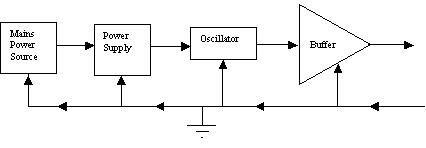
In the Blog entitled Why Electronic Designs Produce EMI Part 1, we discussed why radiated emissions occur in electronic designs.  A simple way to visualize electronic signal current forward and return paths was provided, and mismatched signal path impedance was briefly mentioned as one reason for signals to radiate. In this article, the significance of signal path impedance is described in greater detail.

We can start by asking the question, what kind of signal path will not radiate? Mathematics aside, the simple answer is that a signal path that matches source, path, and destination impedances will not radiate. Here is a simple illustration of a matched impedance signal path:

matched impedances

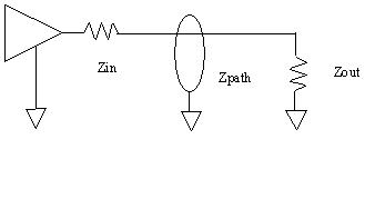
In the above illustration, if Zin=Zpath=Zout across the entire spectrum of frequencies from DC to light and beyond, almost any signal which is sourced from the buffer will not radiate. Why not? Because all of the energy that is sourced from the buffer will be delivered to the load. What happens if there is a mismatch along the way? The simple answer is that mismatched impedances cause signals to reflect, which equates to ringing, which results in radiated noise. This is as true for high speed communications signals as it is for power supply outputs.

How much ringing will there be and at what frequencies? This depends on how much impedance mismatch occurs in the path, how much energy is being transferred, and what the resonant length of the path is.

In both high speed data and power supply applications, circuits are generally designed to have very low impedance at the source drivers, and very high impedance at the destination loads. Also in both high speed data and in power supplies, very sharp edges on switched signals are considered desirable because sharp edges with a lot of energy result in fast data transfer and maximum efficiency switching supplies. Unfortunately, these two conditions also create an ideal environment for signal reflections, especially at high frequencies.

Why do mismatched impedances reflect? Imagine a floodgate opening, and downstream a huge rock blocking the river. What will happen when the current reaches the rock? Water will splash, of course, it will bounce back or reflect into the oncoming stream of water. Water might even splash beyond the edges of the river.

Why do sharp edges result in reflections? The spectral content of a square wave contains odd harmonic signals that can go to very high frequencies. This is why processors operating with a 10 MHz clock or switching power supplies with a 400 kHz clock can produce 250 MHz noise, because of the amount of energy used in switching creates fast rising and falling edged signals. Even a DC switch can produce momentary reflections up to very high frequencies.

So, what does this all have to do with blocked or open return paths described in the previous blog? Even reflected energy seeks the path of least resistance, whether it is reflecting towards the source or the load. If the path of least resistance is a radiated path back to the source supply rather than the circuit board or cable signal / ground path, the reflected energy will radiate.

At Sunrise Electronic Innovations we have decades of experience in designing emissions compliant electronic products. We help customers to reduce emissions on existing products and we provide design and layout review and educational services to improve and cost reduce products. To gain the benefit of our experience, give us a call at 678-358-8775.


EMC Compliance 2015

I just want to take a moment to thank you for your interest and your business in 2014, and wish you well in the coming year.

cropped-sunrise-over-earth_2.jpg2014 was my first year trying in earnest to get out there and market the Sunrise business, and I really appreciate the gracious way I was received by many of you as I visited and shared advice, flyers, business cards, and most recently blogs.

As you know, I specialize in EMC oriented product design and layout reviews, product prescreen, and trouble shooting EMC issues in electronic products. I’m grateful for the opportunities I had to help customers in 2014, and I hope more customers will consider including me as part of their product design cycle in 2015.

In addition to EMC specific product review and testing, I’m glad to have been of service in test and certification plan development last year, especially with regard to CE and other worldwide market certification planning. This also included electronic product pre-auditing for compliance to safety standards.

I’m also grateful for the collaborative partnerships I have with NVLAP and A2LA certified test labs and PCB design and fabrication houses. I’m especially grateful to Gordon Helm at AHD, located in Southwest Michigan, for continuing to utilize me as his NVLAP ISO 17025 Quality Manager. I’m also grateful to Russ Martin and Jeff Woods at ACS Test Labs in Buford Georgia, and David Schramm at SGS in Suwanee, Georgia for the resources, referrals, and overall support.

I hope that the economy continues to improve and we all enjoy a healthy and successful year in 2015. Please remember Sunrise Electronic Innovations for your EMC Compliance planning, design, prescreen, and trouble shooting needs.

Take Care,

Dave Miller, NCE
Sunrise Electronic Innovations LLC
678-358-8775
dave@emcdesigner.com

Certifying Unlicensed Transmitter Products in Canada

“We are selling our part 15 unlicensed transmitter products successfully in the US.   Our certification testing, reports, declarations, and labels are all consistent with FCC requirements, and we have an interest in selling our products in Canada. What do we need to do?”industrycanada

Canadian electronic product compliance law is fairly consistent with US law, which makes selling electronic products into Canada relatively straight forward. While in the US unlicensed transmitters need to be certified with the FCC, in Canada unlicensed transmitters need to be certified through “Industry Canada” authorities.

While in the US, product certification requires using independent “Telecommunication Certified Body” (TCB) contractors, engineers on staff within Industry Canada validate and certify product documentation directly. This means that certified test labs in the US who are registered with Canada can file certification data and documentation directly.

While US and Canadian emissions data and reporting requirements are similar, they are not exactly the same. For example, Canadian law requires that signal bandwidth be measured and reported in a slightly different manner. Canadian laws are also more specific with regard to instrument settings when measuring emissions.   Additionally, documentation filed with Canada generally needs to cite applicable Canadian laws and standards. The bottom line is that reports written for FCC compliance usually require some “tweaking” to meet Canadian requirements.

With regard to product certification, Canadian law requires that a “Canadian Contact” be included with the registration. A Canadian Contact is a company that is willing to assume direct contact responsibilities within Canada for any questions or complaints initiated after the product is certified.

Also, Canadian labeling requirements apply in addition to FCC, and user manual documentation needs to include compliance information in both French and English languages.

At SEI, we can help guide you through the certification process in the US, Canada, Europe, and beyond. One of the services we provide is product test planning, to help bring your product to market as quickly and as cost efficiently as possible. Give us a call to request a quote for product prescreen and debug, test and certification planning, and certification testing and report services through AHD or a certified test lab of your choice.

Why Electronic Products Produce EMI Part 1

Electronic designers may avoid considering electromagnetic compatibility because their exposure to electromagnetic field theory was so mathematically intensive. While mathematical models are important, focusing on the math can distract a person from appreciating the practical aspects of how electromagnetic fields behave.

In my experience, the easiest way to understand EMI is to think of water. Water seeks the path of least resistance, and water wants to return to its source.

In EM terms, what is a source? Any place where current originates. A buffer, a power supply, a driver, or even a bypass capacitor, an inductor, or ferrite bead can be thought of as a current source.

Unlike water, when electrical current flows, it generates an electromagnetic field. And the EM field that current generates in turn influences the path along which the current flows.

Ideally, in electronic circuits, all return currents follow paths back to their sources that match the paths that the currents originate from. Consider the diagram below:

figure1Figure 1: Optimal Current Paths

The arrows indicate both primary current flow paths and return current flow paths through ground. When return current flows along a path that matches the source path, the EM fields generated by the current flow cancel each other, and the circuit does not create Electromagnetic interference. Another way to look at it is that all the current energy stays within the intended pathways.

Like water, electric current energy follows the most efficient path back to its source. If the intended pathway is not the most efficient route for return current to follow, the electric fields generated by the forward and return currents will choose a more efficient path, and emissions will result.

Now consider the figure below, which illustrates a problematic return path in the buffer circuit described above:

figure2

Figure 2: Problematic Current Paths

Notice in figure 2 how the most efficient return path for the current being sourced by the buffer is no longer the short path back to the buffer, but rather a long looped path through earth or chassis ground and the mains power source.  When tested for emissions, the above illustration may produce either conducted or radiated emissions, depending on the frequency characteristics of the buffer sourced current.

Why would electrical energy choose a long path rather than the intended short path? This is where a little math may be required, or at least an understanding of what the math predicts. One reason might be that the longer path happens to match a resonant wavelength of some harmonic frequency of the alternating buffer current. Another reason might be that the intended return path presents a high impedance at the offending frequency and actually blocks the return current. Mismatch between the buffer circuit source, path, and destination impedances can be a factor as well, causing undesirable reflections in the buffer sourced current.

Whatever the cause for the undesirable emissions, understanding the behaviors of electromagnetic fields can help a designer to “design out” potential EMC issues prior to testing. Looking at a design as a series of current sources that require adequate return paths can assist in this understanding.

Part of our job at Sunrise Electronic Innovations includes educating our customers while doing design reviews and product pre-screen testing. As we educate our customers, their designs improve to the point that little to no modification is required for passing certification testing. To gain the benefit of our experience, please give us a call at 678-358-8775.

Using Certified Transmit Modules in Electronic Products

Incorporating modules that have already been FCC certified can be a good way to introduce wireless functionality into a product line. While the use of pre-certified modules simplifies the compliance testing process, several factors must be considered.

Certified modules have grant conditions associated with them. The grant conditions for a device are an_rko_radio_picture___extended___rocky_horror_by_deviever-d5b7ex8supposed to be documented in the device user manual, but they can also be found by looking up the device FCCID Form 731 on the FCC website. Grants usually include restrictions on antennas, operational duty cycle, and the intended usage model of the device, including collocation of the device with other transmitters and end user exposure to rf signals.

At minimum, an end product incorporating a wireless module still requires emissions testing, an emissions report, and appropriate FCC labeling prior shipping in US. If the module is used in a manner consistent with the module’s grant conditions, FCC part 15 subpart B unintentional radiator testing and documentation is required. FCC regulation 15.212 describes how labels must identify certified modules used internal to the end product.

If the module is collocated with another transmitter closer than either transmitter grant allows, or if the module is used in a manner inconsistent with its grant (i.e a mobile device grant used in a user extremity exposure configuration), additional testing and documentation must be provided to prove that EMC and end user rf exposure limits are not exceeded. EMC testing would include scanning for intermodulation noise products, and at minimum SAR exclusion thresholds for the collocated transmitters must be calculated. See KDB 447498 D01 for information about SAR testing and exclusion requirements.

If testing and calculations prove that transmitter performance is not degraded, the testing described above would be consistent with a Class 1 Permissive Change, which does not require filing with the FCC. Documentation for Class 1 configuration changes should be forwarded to the module manufacturers.   See FCC regulation 2.1043 and KDB 178919 for more information regarding Permissive Changes.

If a module is modified in a manner that increases its output power, a new FCCID is required for the device. This can be filed by either the end product manufacturer or the module manufacturer. A full suite of transmit performance tests are required specific to the operating frequency and mode of the module.

If a module is used in a manner that is inconsistent with the grant and degrades the performance of the module, including changes to the antenna or operational parameters, then a class 2 permissive change may be necessary for the module.

Class 2 permissive changes are required to be filed by the certified module manufacturer. If the module manufacturer does not wish to file the change, the end product manufacturer can request a cover letter from the module manufacturer granting permission to file the change. If the module manufacturer is not willing to give the end product manufacturer permission to file the change, then the end product manufacturer must obtain a new FCC ID. For more information regarding transmitter module equipment authorization, see the FCC KDB 996369 document.

In conclusion, while use of certified transmit modules in end user products can simplify the compliance process, care must be taken with regard to grant restrictions associated with the module. Factors such as antenna usage, operational duty cycle, intended usage model of the device, and collocation of the device with other transmitters all affect what testing and documentation is required before marketing a device in the US.

The contributions towards this discussion from Jeff Woods CB Manager at ACS test labs and Gordon Helm at AHD test lab are greatly appreciated. Feel free to comment on this and other upcoming blogs. The interpretation of rules and regulations with regard to EMC compliance test rules are often conflicting and confusing, and certainly warrant discussion.